- 您现在的位置:买卖IC网 > Sheet目录1201 > CDB5467U (Cirrus Logic Inc)BOARD EVAL FOR CS5467 ADC
�� �
�
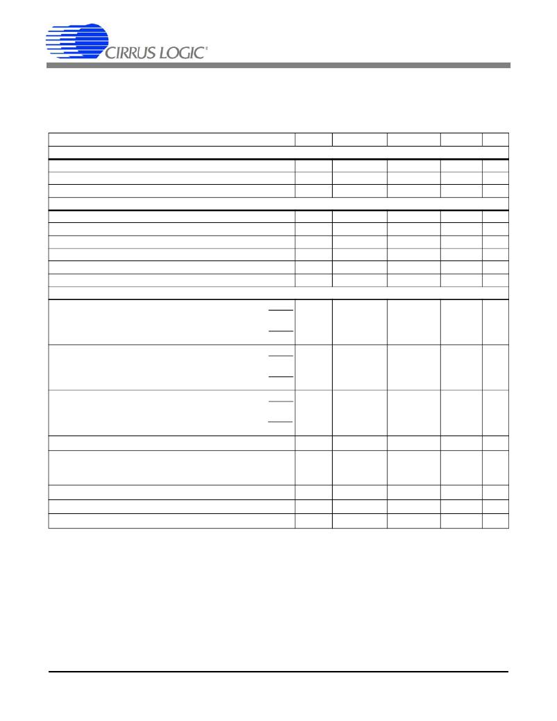
�CS5467�
�DIGITAL� CHARACTERISTICS�
�?�
�?�
�?�
�?�
�Min� /� Max� characteristics� and� specifications� are� guaranteed� over� all� Recommended� Operating� Conditions� .�
�Typical� characteristics� and� specifications� are� measured� at� nominal� supply� voltages� and� TA� =� 25� °C.�
�VA+� =� VD+� =� 5V� ±5%;� AGND� =� DGND� =� 0� V.� All� voltages� with� respect� to� 0� V.�
�DCLK� =� 4.096� MHz.�
�Parameter� Symbol�
�Min�
�Typ�
�Max�
�Unit�
�Master� Clock� Characteristics�
�Master� Clock� Frequency�
�Master� Clock� Duty� Cycle�
�CPUCLK� Duty� Cycle�
���DCLK�
�2.5�
�40�
�40�
�4.096�
�-�
�-�
�20�
�60�
�60�
�MHz�
�%�
�%�
�Filter� Characteristics�
�Phase� Compensation� Range�
�Input� Sampling� Rate�
�(60� Hz,� OWR� =� 4000� Hz)�
�DCLK� =� MCLK/K�
�-5.4�
�-�
�-�
�DCLK/8�
�+5.4�
�-�
�°�
�Hz�
�Digital� Filter� Output� Word� Rate�
�High-pass� Filter� Corner� Frequency�
�(Both� channels)�
�-3� dB�
�OWR�
�-�
�-�
�DCLK/1024�
�0.5�
�-�
�-�
�Hz�
�Hz�
�Full-scale� DC� Calibration� Range� (Referred� to� Input)� (Note� 14)� FSCR�
�Channel-to-channel� Time-shift� Error�
��25�
�-�
�1.0�
�100�
�%FS�
�μs�
�Input/Output� Characteristics�
�High-level� Input� Voltage�
�All� Pins� Except� XIN� and� SCLK� and� RESET�
�XIN�
�SCLK� and� RESET�
�V� IH�
�0.6� VD+�
�(VD+)� –� 0.5�
�0.8� ?� VD+�
�-�
�-�
�-�
�-�
�-�
�-�
�V�
�V�
�V�
�Low-level� Input� Voltage� (VD� =� 5� V)�
�All� Pins� Except� XIN� and� SCLK� and� RESET�
�XIN�
�SCLK� and� RESET�
�V� IL�
�-�
�-�
�-�
�-�
�-�
�-�
�0.8�
�1.5�
�0.2� ?� VD+�
�V�
�V�
�V�
�Low-level� Input� Voltage� (VD� =� 3.3� V)�
�All� Pins� Except� XIN� and� SCLK� and� RESET�
�XIN�
�SCLK� and� RESET�
�V� IL�
�-�
�-�
�-�
�-�
�-�
�-�
�0.48�
�0.3�
�0.2� ?� VD+�
�V�
�V�
�V�
�High-level� Output� Voltage�
�I� out� =� +5� mA�
�V� OH�
�(VD+)� -� 1.0�
�-�
�-�
�V�
�Low-level� Output� Voltage�
�I� out� =� -5� mA� (VD� =� +5V)�
�I� out� =� -2.5� mA� (VD� =� +3.3V)�
�V� OL�
�-�
�-�
�-�
�-�
�0.4�
�0.4�
�V�
�V�
�Input� Leakage� Current�
�3-state� Leakage� Current�
�Digital� Output� Pin� Capacitance�
��I� in�
�I� OZ�
�C� out�
�-�
�-�
�-�
�±1�
�-�
�5�
�±10�
�±10�
�-�
�μA�
�μA�
�pF�
�Notes:� 10.� All� measurements� performed� under� static� conditions.�
�11.� If� a� crystal� is� used,� XIN� frequency� must� remain� between� 2.5� MHz� -� 5.0� MHz.� If� an� external� oscillator� is�
�used,� XIN� frequency� range� is� 2.5� MHz� -� 20� MHz,� but� K� must� be� set� so� that� MCLK� is� between�
�2.5� MHz� -� 5.0� MHz.�
�12.� If� external� MCLK� is� used,� the� duty� cycle� must� be� between� 45%� and� 55%� to� maintain� this� specification.�
�13.� The� frequency� of� CPUCLK� is� equal� to� MCLK.�
�14.� The� minimum� FSCR� is� limited� by� the� maximum� allowed� gain� register� value.� The� maximum� FSCR� is�
�limited� by� the� full-scale� signal� applied� to� the� input.�
�15.� Configuration� register� (� Config� )� bits� PC[6:0]� are� set� to� “0000000”.�
�10�
�16.�
�The� MODE� pin� is� pulled� low� by� an� internal� resistor.�
�DS714F3�
�发布紧急采购,3分钟左右您将得到回复。
相关PDF资料
CDB5560-2
DEV BOARD FOR CS5560 W/SE INPUT
CDB5571-2
DEV BOARD FOR CS5571 W/SE INPUT
CDB8422
BOARD EVAL FOR CS8422 RCVR
CDB8952T
BOARD EVAL FOR CS8952
CDCE906-706PERFEVM
EVAL MOD PERFORMANCE CDCE906/706
CEVAL-033
BOARD EVAL FOR CVCO33 .3"X.3"
CF37S
COVER FLANGE 37POS FEMALE
CG0402MLC-05LG
SUPPRESSOR ESD 5VDC 0402 SMD
相关代理商/技术参数
CDB5471
制造商:Cirrus Logic 功能描述:Tools Development kit Kit Con
CDB5480U-Z
功能描述:电源管理IC开发工具 CS5480 Eval Board
RoHS:否 制造商:Maxim Integrated 产品:Evaluation Kits 类型:Battery Management 工具用于评估:MAX17710GB 输入电压: 输出电压:1.8 V
CDB5484U-Z
功能描述:电源管理IC开发工具 CS5484 Eval Board
RoHS:否 制造商:Maxim Integrated 产品:Evaluation Kits 类型:Battery Management 工具用于评估:MAX17710GB 输入电压: 输出电压:1.8 V
CDB5490U-Z
功能描述:电源管理IC开发工具 CS5490 Eval Board
RoHS:否 制造商:Maxim Integrated 产品:Evaluation Kits 类型:Battery Management 工具用于评估:MAX17710GB 输入电压: 输出电压:1.8 V
CDB5501
制造商:Cirrus Logic 功能描述:EVAL BOARD FOR CS5501 - Bulk
CDB5503
制造商:Cirrus Logic 功能描述:EVAL BOARD FOR CS5503 - Bulk
CDB5504
制造商:CIRRUS 制造商全称:Cirrus Logic 功能描述:Low Power, 20-Bit A/D Converter
CDB5505
制造商:Cirrus Logic 功能描述:EVAL BD FOR CS5505 - Bulk